welcome to nanospective
NanoSpective is an advanced materials characterization services provider with facilities located in the Central Florida Research Park (adjacent to UCF). We offer comprehensive solutions for physical analysis with applications in intellectual property, hardware cybersecurity, root cause failure analysis, quality control, materials research and beyond. With lineage tracing back to our days at Bell Labs, we have decades of experience in process level semiconductor/IC characterization from packaging to transistors to interconnect to atomic resolution imaging and spectroscopy.
We are an advanced materials characterization company, with expertise in the science of materials. We understand the landscape of nanotechnology & microelectronics
Our high-performance teams combine client consultation and critical thinking to deliver custom-tailored commercial analytical services with academic level attention to detail
Our culture highly prioritizes excellence in work product, client support, teamwork, mentoring and community involvement
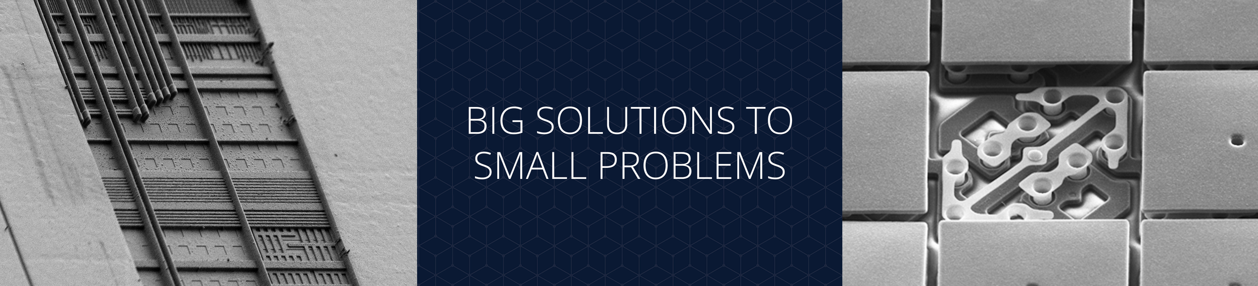
our Vision is to be the best custom analytical services company in the world
CORE COMPENTENCIES

-
Teardown and depackaging of IC, MEMS, LED, image sensors, turbines, mechanical parts; mechanical sectioning and polishing, wet and dry etching, focused and broad ion beam milling
-
Sub-micrometer precision material removal and deposition. Used for stand-alone ion probe microscopy as well as TEM, SEM, APT and SIMS sample preparation
-
Non-contact 3D metrology; high-resolution optical imaging combined with nanometer scale surface roughness and film thickness measurements
-
Direct visual observation (up to ~1000X); Characterization based on morphology, color, opacity and optical properties; Illumination sources including white light, infrared and laser
-
High magnification imaging (up to ~200kX) and elemental analysis using energy dispersive spectroscopy (EDS)
-
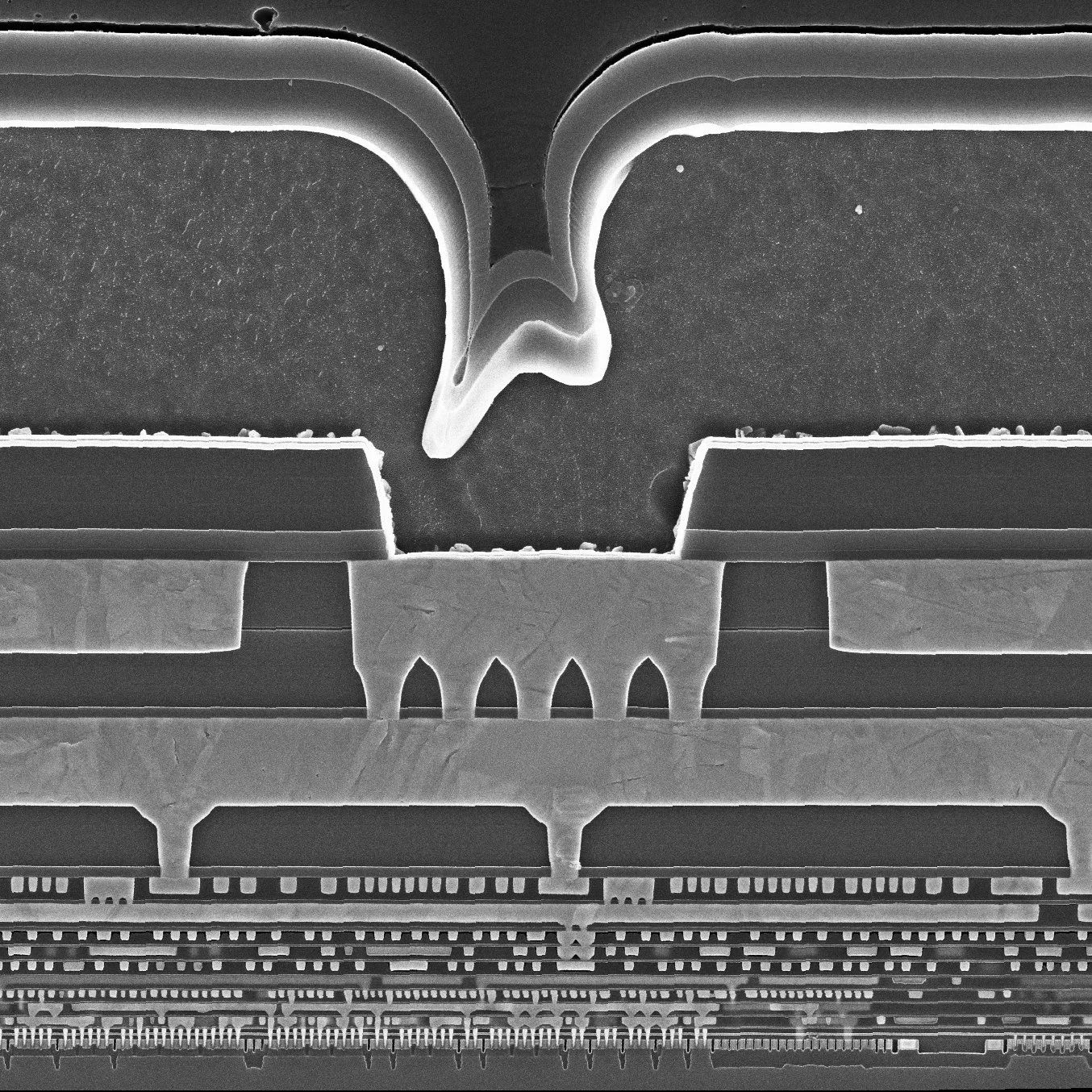
Ultra high-resolution imaging (>1.5MX), conventional and 4D-STEM diffraction analysis to characterize microstructure. Elemental and chemical information from EDS and electron energy loss spectroscopy (EELS)
Additional Characterization Techniques are Available
WE DELIVER CUSTOM TAILORED SOLUTIONS
Whether the work is in intellectual property, failure analysis, quality control or research and development, NanoSpective provides a range of analytical services to meet our clients’ needs
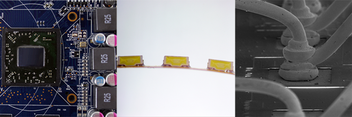
• Microelectronics: State of the art IC, Memory and Logic, MEMS, Imagers, Sensors, etc.
• Display Technology, LCD, TFT, LED, etc.
• Advanced Packaging & Printed Circuit Board
• Photonics & Optoelectronics
• Coatings and Thin Film
• Metals, Composites and Ceramics
• Communications, Wireless & RF


WE VALUE OUR CLIENTS
Our company centers on both client and employee needs, delivering full-spectrum materials characterization solutions for intellectual property, cyber security, failure analysis, quality control, and materials research
We provide our clients with specialized technical expertise. Whether you have a single analysis or ongoing projects, our scientists will provide a custom-tailored analytical plan to fit your requirements. An excellent work product and superior client support are our top priorities at NanoSpective
For every new project, we provide a customized quote detailing the project specifications. Our scientists will consult with you and will provide ongoing expertise until the project is completed